Project overview
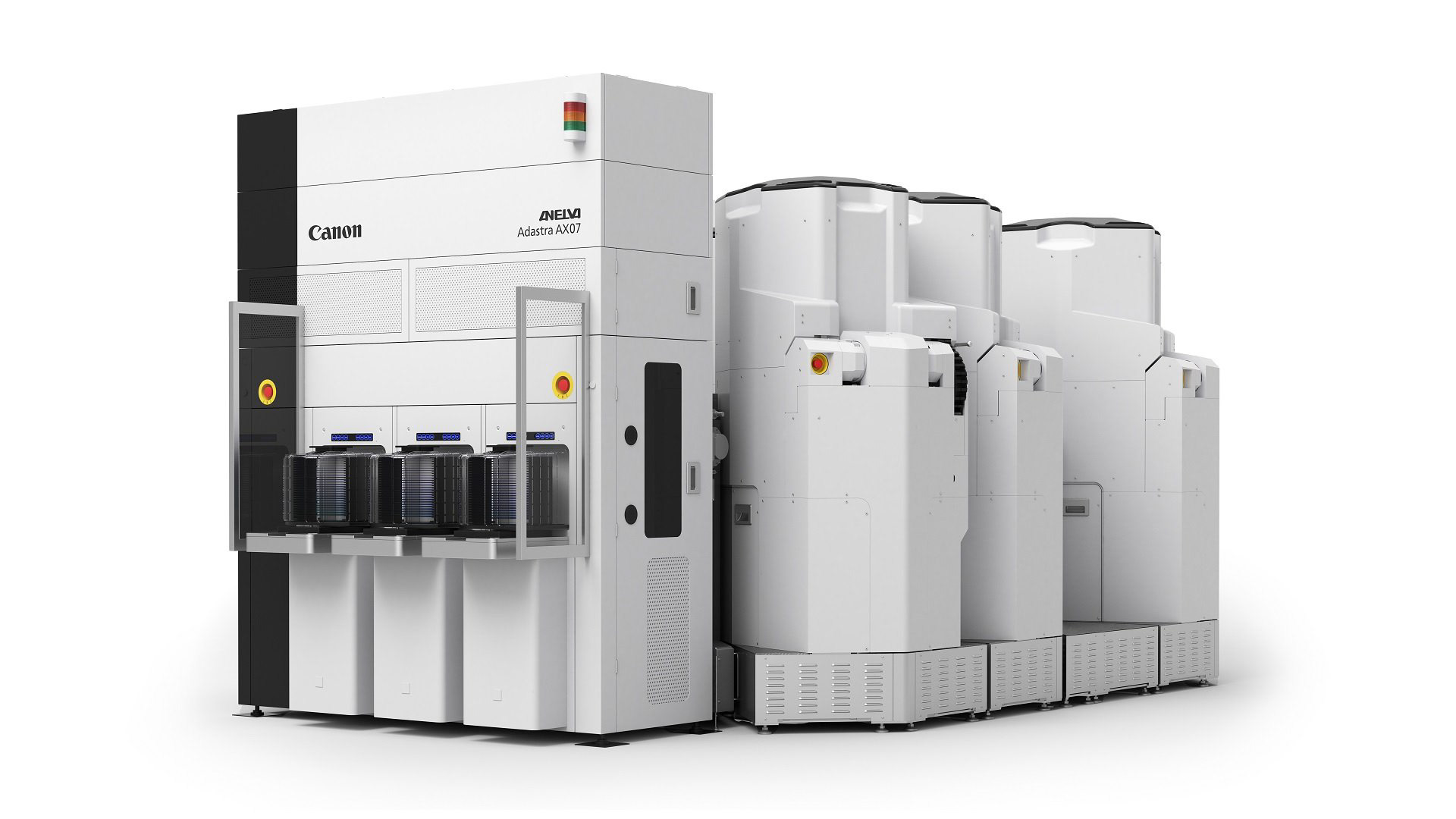
Adastra AX07 is a sputtering system platform developed by Canon ANELVA for semiconductor and electronic component manufacturing.
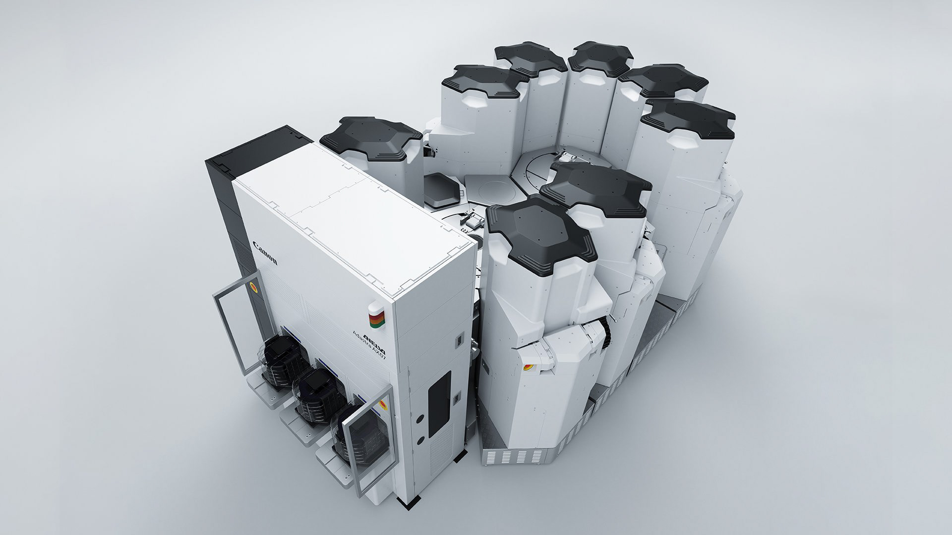
We developed the equipment’s exterior design around its expandable architecture, which arranges multiple process modules around a central core. The design accommodates complex internal mechanisms while addressing enclosure manufacturing requirements and maintenance access.
By considering equipment configuration, ease of operation and manufacturability together, we established a distinctive design language for this semiconductor manufacturing platform.


Awards
iF DESIGN AWARD 2025 — GOLD
GOOD DESIGN AWARD (JPN) 2024— GOLD PRIZE
55th Machine Design Award IDEA, 2025 — Grand Prix
Design Concept / Translating Equipment Architecture into a Distinctive Identity
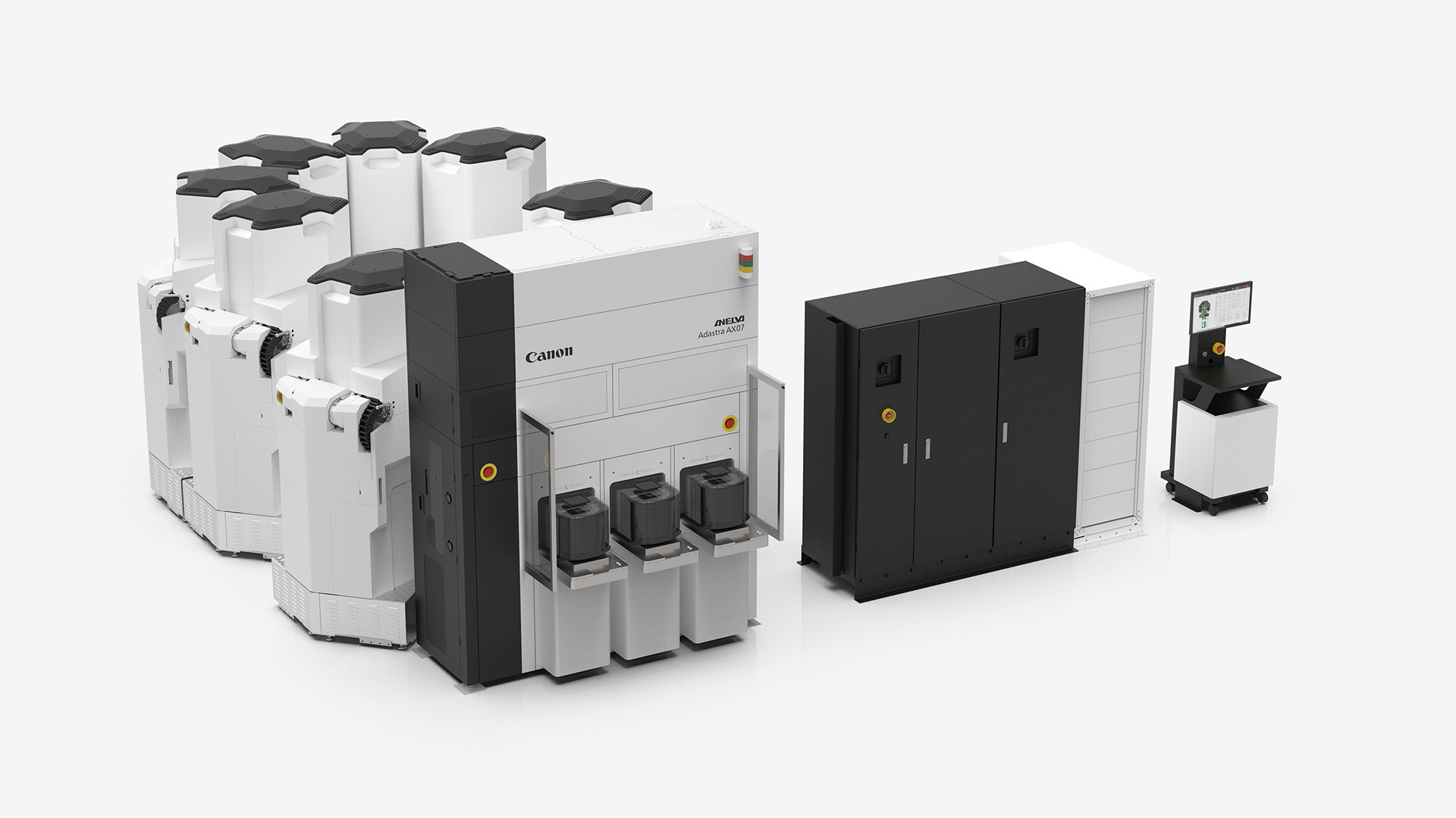
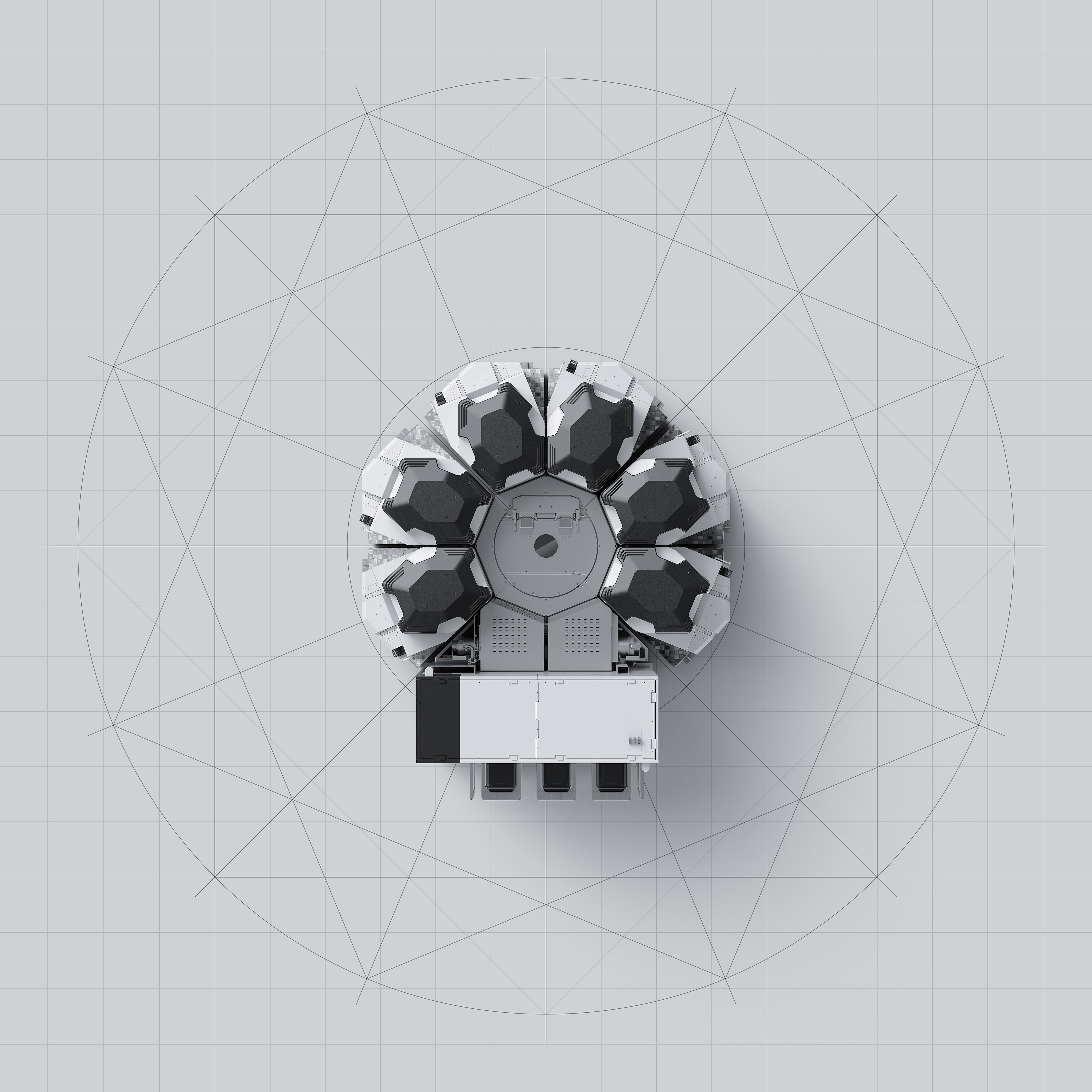
The geometry of the central core and surrounding process modules informed the equipment’s overall form, establishing a consistent visual identity across the platform.
The enclosure integrates the complex arrangement of piping, cabling and internal mechanisms into a clear, coherent silhouette. Contrasting white enclosure panels and black upper covers articulate the equipment’s functional layout and convey its advanced technical character.
Modular Architecture / An Enclosure System Designed for Expansion and Manufacture
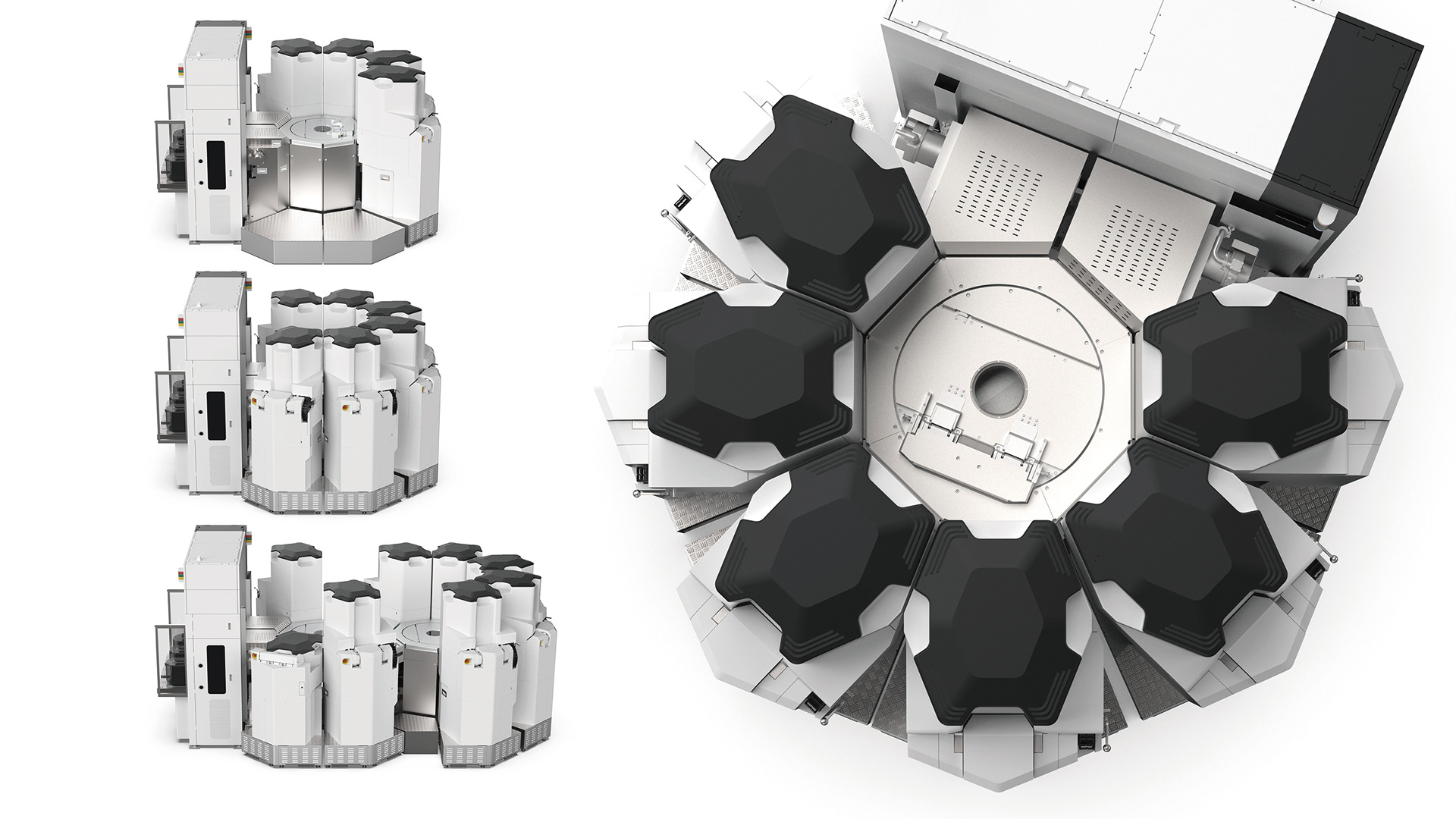
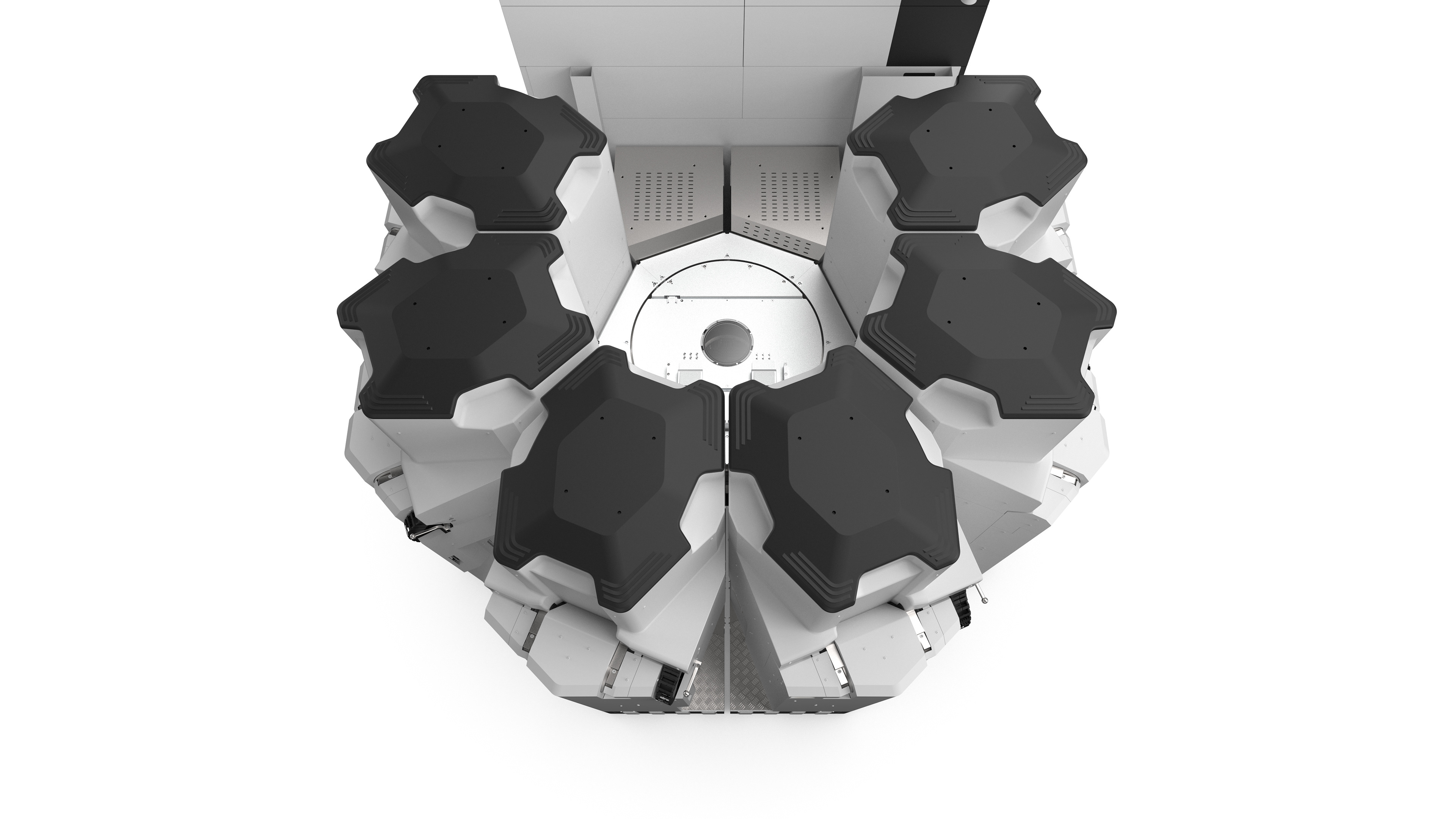
Adastra AX07’s platform architecture arranges multiple process modules radially around a central transfer core. Modules can be selected and reconfigured to suit different applications, allowing the platform to support equipment configurations from R&D through volume production.
We incorporated the faceted geometry of this architecture into the enclosure design, using the spaces between adjacent modules for maintenance access. The enclosure system maintains a consistent visual language while preserving working space and the clearances required to open and close the upper covers.
The design also addresses the fabrication and assembly constraints of large enclosure components. Cover geometry, panel divisions and fastening methods were developed together to create an enclosure system suitable for repeatable manufacture.
Ergonomics & Maintenance / Serviceability and Safety in the Cleanroom
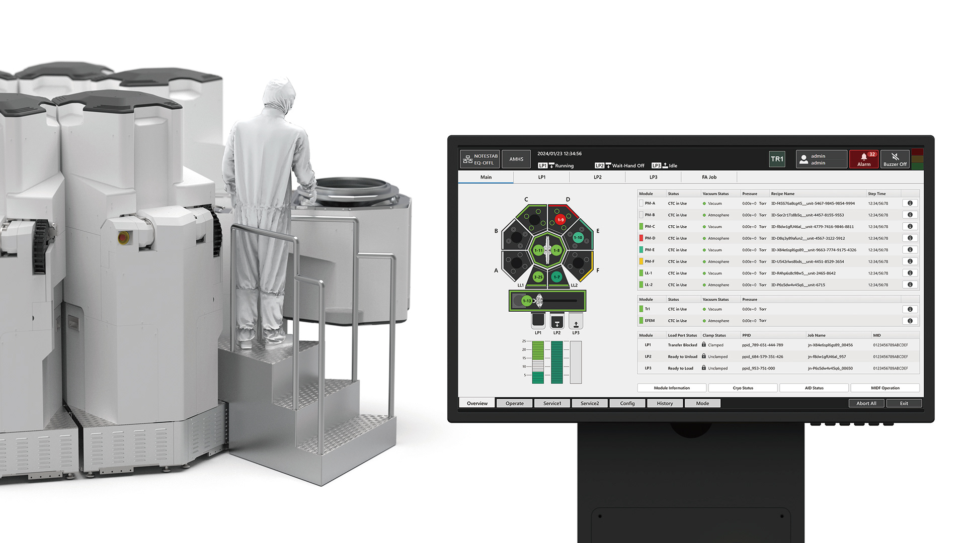
Our designer entered the cleanroom in clean-suits to assess the working environment firsthand. Direct observation and operator interviews helped map maintenance procedures and identify the physical demands of each task.
The ergonomic study addressed conditions such as replacing heavy components and working at elevated positions, including the geometry of handholds and the postures required during servicing.
Protective covers shield sharp internal-parts' edges and heat sources, while surfaces that operators may contact are shaped with safety in mind. These design details improve usability, operator safety and serviceability.
Detail Design / Integrating Moving Mechanisms with the Enclosure
The black upper covers express Adastra AX07’s integrated architecture and advanced technology, giving its expandable module configuration a recognizable visual identity. Their contrast with the white enclosure makes the equipment’s functional organization easier to read.
Around the cable carriers, the enclosure geometry accommodates the full range of motion and cable routing while maintaining a coherent exterior. These mechanical requirements inform the equipment’s overall design language, bringing functional constraints and industrial design into alignment.
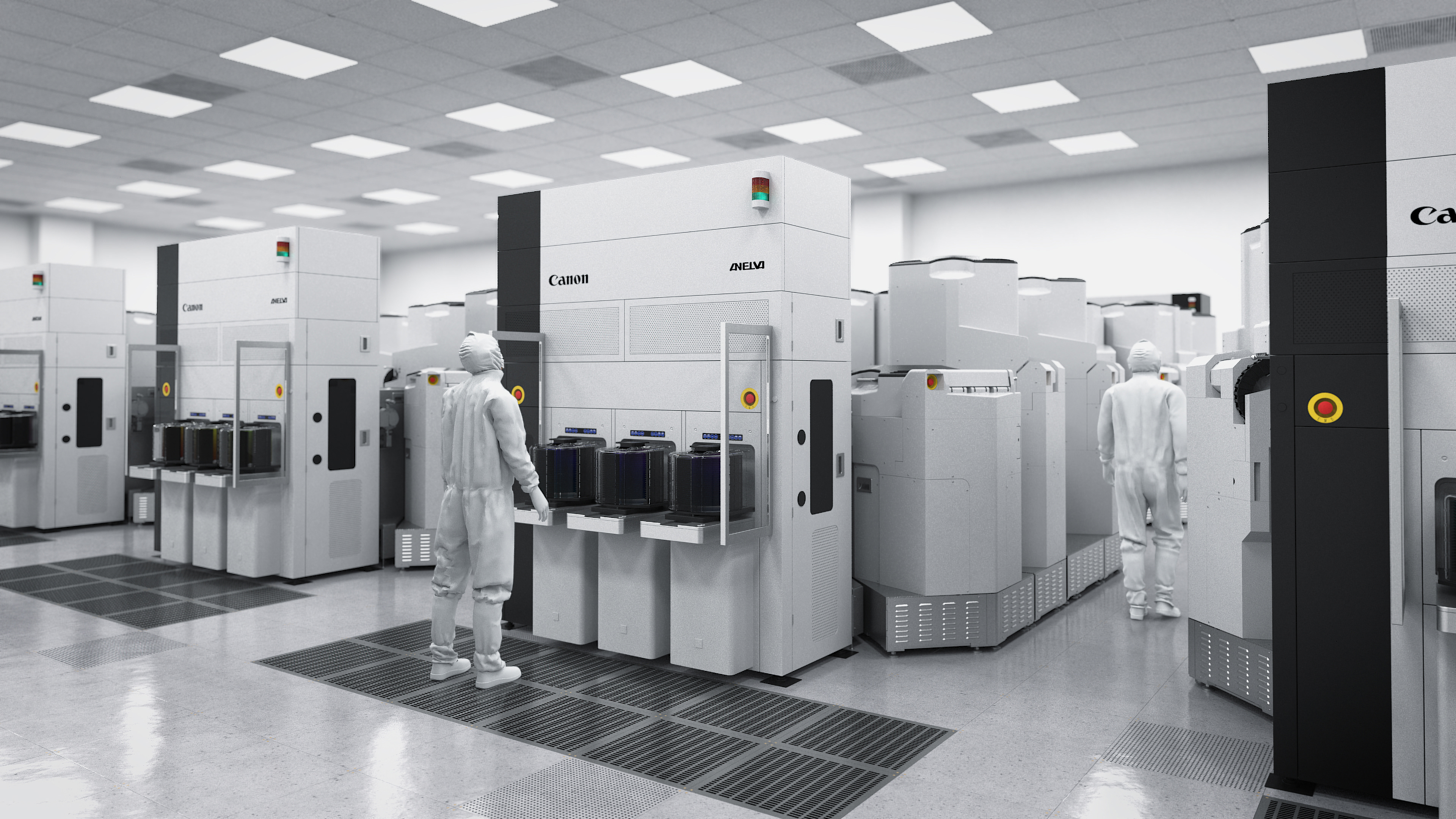
Space Efficiency / Maximizing the Use of Cleanroom Floor Space
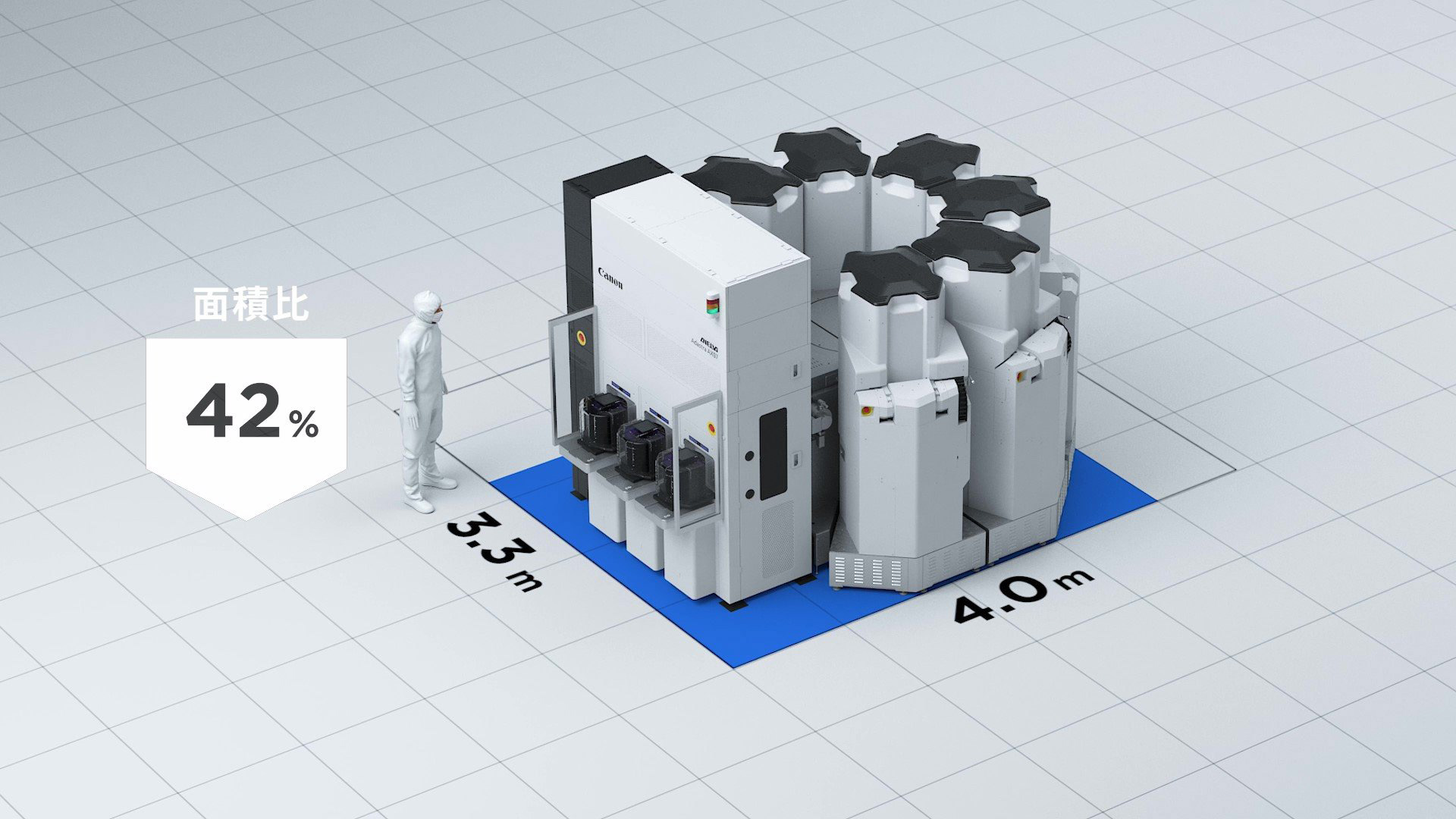
In cleanrooms housing multiple semiconductor manufacturing systems, efficient use of floor space is a critical consideration alongside the performance of each tool.
By integrating process modules around a central core, Adastra AX07 reduces the equipment footprint by approximately 42% compared with the previous system. This compact architecture makes more efficient use of limited cleanroom space and supports greater production capacity per unit of floor area.

Project: Adastra AX07
Category: Semiconductor Manufacturing Equipment
Product: Sputtering System Platform
Scope: Product Design / Industrial Design / Enclosure Design / Ergonomics / Design for Manufacturing
Client: Canon ANELVA Corporation
Photo Credit: Canon ANELVA Corporation
Category: Semiconductor Manufacturing Equipment
Product: Sputtering System Platform
Scope: Product Design / Industrial Design / Enclosure Design / Ergonomics / Design for Manufacturing
Client: Canon ANELVA Corporation
Photo Credit: Canon ANELVA Corporation
Semiconductor & Industrial Equipment Design
We provide industrial design services for complex B2B equipment, including semiconductor manufacturing systems, vacuum equipment and precision industrial machinery.
Our capabilities span enclosure and exterior design, 3D CAD development, color, material and finish (CMF), and ergonomics. We develop designs that work within mechanical engineering constraints and manufacturing requirements.